
Circuit Design on Your Linux Box Using gEDA
A lot of attention—and hype—has focused on bringing traditional office-productivity programs, such as the OpenOffice.org suite, to Linux. However, another important—and far less-hyped—area where Linux's desktop abilities come to the fore is in engineering software, and in particular, CAD (computer-aided design).
Non-engineers tend to think of the term CAD as referring to mechanical design software, and they are partially right. We are used to seeing complicated drawings of mechanical assemblies appearing on computer screens in advertising and television. However, CAD doesn't mean only mechanical design. Electronics designers also long have used computer-based design tools to help them perform their design tasks.
The area of CAD software used for electronics design is typically referred to as EDA, short for electronic design automation. Happily for Linux users, many EDA applications—both proprietary and open source—are now available for Linux. Perhaps the largest and oldest open-source project is the gEDA Project. The gEDA Project is an active community of hackers who have developed high-quality EDA applications for many different electronic design tasks. In this article, we examine a set of gEDA programs you can use to design your own circuit boards from scratch.
Designing circuits using EDA tools is analogous to creating software using traditional software engineering tools. That is, rather than using only one program to accomplish a job, electrical engineers will use a wide variety of tools, each tailored to accomplish its particular task efficiently. They use each tool in a sequence as they progress from start to finish through their design work, a concept known as design flow. This concept should be familiar to software engineers who might first use a flowcharting tool, then an editor, followed by a compiler, then a debugger, as they create applications ready for distribution.
Different types of circuit design use different flows. For example, if you work on digital electronics, you might code your design using a hardware description language such as Verilog, and then use a Verilog compiler followed by a waveform analyzer to simulate and analyze it. On the other hand, if you are doing analog circuit design, you might draw your circuit using a schematic capture program, and subsequently use a circuit simulation program, such as SPICE, to verify its correctness before prededing to create a PC board. Other, more-complicated designs might require additional steps in the design flow.
In this article, our interest is to create a garden-variety printed circuit board (PCB). To create a simple circuit board using any EDA toolset—whether proprietary or open source—the design flow looks like this:
Gather information about your design's requirements, as well as find data sheets for available parts.
Create a high-level block diagram of your design, using either paper and pencil or a general-purpose drawing program such as Dia.
Enter your detailed design into the computer, and draw its schematic using a special-purpose schematic capture program.
Netlist your design's schematic, meaning that you export a so-called netlist that captures all your design's components and connections in a special-purpose file format.
Read the netlist into a layout editor, which is a special-purpose drawing program for creating PCBs. Use the layout editor to create a drawing of your PC board's physical layout.
Export Gerber files from your layout program. The Gerber files are industry-standard files that describe your PCB to your PCB manufacturer.
Send the Gerber files to a PCB fabricator.
Receive your freshly manufactured PCBs, populate them with components and test them out.
At any point in this flow, you might have to go back and repeat a step if you find an error in a proceeding step. Again, this is similar to software engineering, where you have to go back to edit and recompile your program if you find that it has a runtime error. The only difference is that if you take a PCB design to its completion by ordering boards, and then you find a design error, you're stuck with a batch of bad boards—you can't simply delete your work and recompile.
The gEDA Project was originated by Ales Hvezda in 1998. After graduating from the University of New Mexico, he became interested in robotics. Ales wanted to design circuits for robots using his Linux box, but found that no suitable applications running on Linux existed. Consequently, like so many open-source developers active in other areas, he felt the itch to write his own EDA suite. Ales scratched the itch by writing a schematic capture program and a rudimentary netlister. He also created a Web site to share his efforts, which he named the gEDA Project, because he wanted to release his EDA creations under the GPL.
Very quickly, a small team of developers joined him and started patching and adding to the gEDA tools. Others started contributing tools of their own, some of them modest design utilities and others major software projects in their own right. In the latter category fall the ngspice Project, which aims to develop an open-source implementation of the popular analog simulator SPICE; Gnucap, an analog/digital circuit simulator; and Icarus Verilog, a tool for digital logic generation and simulation. Finally, a very important allied program is pcb—the printed circuit board layout editor.
Because his idea was met with such enthusiasm, and so many tools allied themselves with the gEDA Project, Ales decided to rename his original suite of tools gEDA/gaf, an acronym for gschem and friends. Meanwhile, the term gEDA Suite has come to designate the entire ensemble of open-source EDA tools that have allied themselves with the gEDA Project. A main distinction between gEDA/gaf and the other tools is that the gaf tools tend to be used at the front-end stages of a design, while the other tools are used in later stages.
Since he started it in 1998, gEDA/gaf has grown to a full suite of front-end EDA applications. Besides the core programs gschem and gnetlist, there are almost two-dozen contributed utility programs, including an attribute manager, a symbol checker, an refdes generator (or component numberer), symbol generators and file format conversion utilities. Meanwhile, the various back-end tools, such as pcb, ngspice and Gnucap have also evolved and matured, enabling a variety of different flows adapted to different design types. Currently, the design tools in the open-source gEDA Suite will support almost any kind of low- to mid-level electronic design task, offering the same power as tools costing thousands of dollars.
When discussing the future of EDA on Linux with my friends and colleagues, I like to point out that Sun Microsystems became the corporate giant it is today by offering a great platform for engineering design. Linux can follow the same path to greatness because it, too, offers a powerful platform for engineering applications. Engineers are a natural customer base for Linux as they are smart, technology-savvy and actually want to use UNIX-native power tools such as TCL, Perl and Python to automate their work. Commercial EDA vendors have just begun to realize the customer leverage they can get from the Linux platform, and they are moving fast to serve that market. However, open-source developers recognized the importance of Linux to electronic design many years ago, and the maturity of the gEDA Suite is proof of their early insight.
A good way to understand how gEDA is used is to examine its individual pieces in the context of the overall design flow. The first design step involves schematic capture—that is, using a specialized drawing program to draw a schematic representation of your circuit. The gEDA Suite's schematic capture program is called gschem.
gschem is usually invoked from the command line; once started, it opens up a GUI composed of a drawing window surrounded by all the menus and buttons necessary to draw a schematic. gschem, like any schematic capture program, has a number of built-in graphical primitives corresponding to wires, component pins, resistors, capacitors, transistors and other items you need to connect when creating a circuit design. A screenshot of a typical session with gschem is shown in Figure 1.
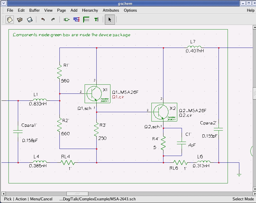
Figure 1. gschem in action. Here is a section of a two-transistor microwave amplifier being drawn in preparation for SPICE simulation.
As for electronic devices, gschem maintains a library of component symbols, which are drawings of individual circuit elements such as resistors, ICs, connectors and anything else you might want to place on your schematic. Each symbol is stored as an ASCII file; when you place a component symbol into your schematic, the corresponding symbol file is opened up and the information contained in it is used to draw the symbol on your screen.
Currently, gschem's symbol library holds more than 2,000 component symbols, including symbols for most common electronic parts. However, engineers commonly need to create new symbols for their designs, because it is likely that not all the parts they want to use are present in the symbol library. Therefore, gschem—like all schematic capture programs—incorporates a symbol editor, which allows users to create and save their own symbols, which they can then use in any design.
gschem understands electrical connectivity, an important property for any schematic capture program. That is, wires (called nets in EDA parlance) know that they can connect only to component pins and other nets. When two nets are connected together, gschem knows to draw a large dot at the connection point, indicating to the user that a connection exists at that point.
gschem enables engineers to attach attributes to each component, which is an important part of creating a design. For example, if you have a 499-ohm resistor in your schematic, gschem lets you place a resistor symbol from the library, double-click on the resistor and then attach a value=499 to the resistor itself. Later, when the design is netlisted, the component's attributes are written into the netlist file and made available for other programs.
Finally, gschem saves your design in a well-documented ASCII format. There are many advantages to ASCII file formats; readers of Linux Journal will appreciate that ASCII files can be parsed and manipulated using scripting languages, including Perl and Python. Scripts facilitate labor-saving design tasks like automated symbol generation and schematic merging. Many proprietary EDA programs do not use ASCII file formats because they are interested in locking in customers. Open-source EDA advocates believe that open file formats are a key superiority of toolsets like gEDA.
After you have captured your schematic, the next step in the design flow is to create a netlist. gnetlist is the gEDA/gaf program used to generate netlists from your schematic files. gnetlist is a command-line utility; when you run it, it generates output netlist files and also displays diagnostic information in your terminal window.
So what's a netlist? A netlist is a file holding your design's connectivity information in a structured format suitable for machine processing. Many different types of netlist exist; each represents a file format optimized for a particular type of subsequent processing. For example, SPICE analog simulators read files written in the SPICE netlist format, which calls out connections between analog components, as well as specifies the values of each component's parameters, such as a resistor's resistance. As another example, netlists used as the input to lay out programs typically hold information about each component's PCB footprint, which is the metalization pattern on the circuit board to which the component is soldered, as well as connectivity information between all component pins.
gnetlist is designed in a unique way. It incorporates a front end written in C that reads and parses your schematic files. Once the read-in is complete, gnetlist invokes a back-end netlist generator written in Scheme. The back end is specific to the desired output netlist. The back end to use is specified via a command-line flag when you invoke gnetlist. gnetlist was designed this way to facilitate easy extensibility. Users who want to create new netlisters simply need to write a Scheme program implementing their desired netlister; they don't need to learn C or fool around with the internals of reading or parsing schematic files.
At the time of this writing, gnetlist can output more than 20 netlist formats. Among the important netlist types output by gnetlist is SPICE. The powerful gEDA SPICE netlister spice-sdb supports the inclusion of vendor SPICE models into your spice netlist. It has proven very popular with EE students worldwide, perhaps because it is well documented in a HOWTO available on the Web. Also, netlisters for several different layout tools exist. Finally, gnetlist is also used for BOM (bill of materials) generation and DRC (design rule checking) using any of several back ends crafted to achieve these goals.
Important to PCB design is the question of how to translate a gschem schematic into a format suitable for layout using the open-source layout program pcb. Although this can be done using gnetlist alone, the procedure is complicated. Therefore, Bill Wilson made a recent contribution to the gEDA Project by writing gsch2pcb, a C utility that wraps gnetlist and outputs the correct files to read into pcb for layout. gsch2pcb is a key addition to the gEDA Suite because it makes the transition from a gschem schematic to a pcb layout easy, and it also illustrates the vibrancy of the gEDA on-line community.
Once the initial layout files are created using gsch2pcb, you can lay out your design. This involves using a layout editor—a specialized drawing program to draw metal tracks, components, drill holes and other structures onto your circuit board. The PCB layout tool used with gEDA is called, appropriately enough, pcb. pcb usually is invoked from the command line; once running, it presents a drawing window accompanied by all the widgets and tools necessary to draw your circuit board. A screenshot of pcb in action is shown in Figure 2.
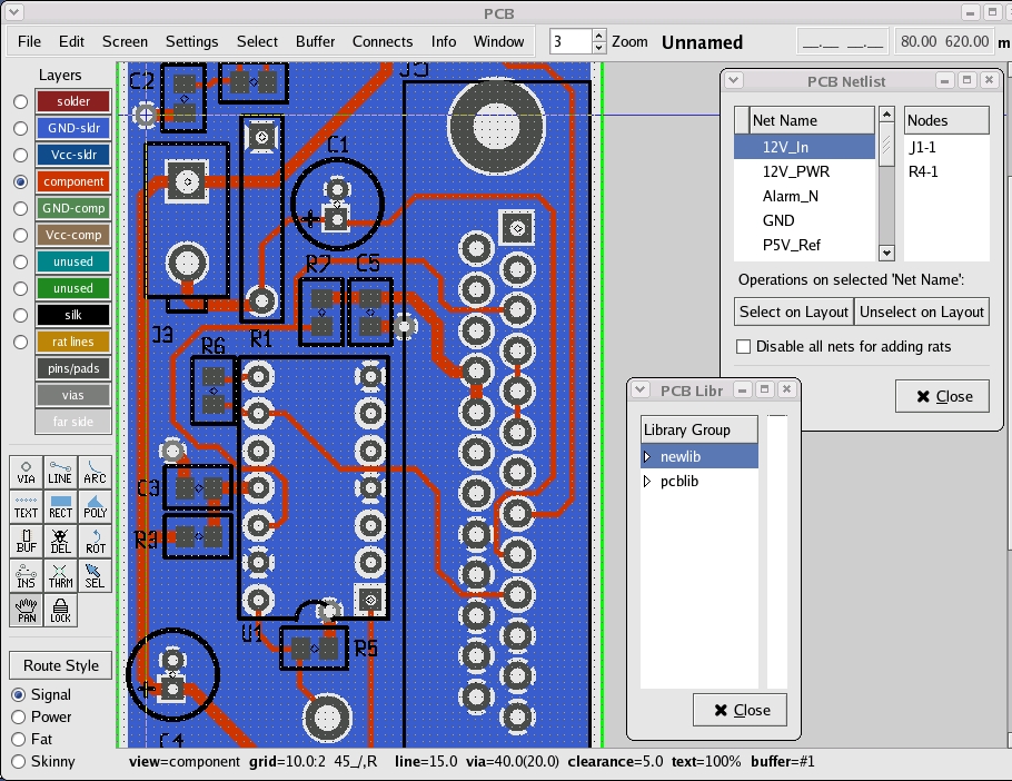
Figure 2. A board layout in pcb. The red lines represent metal traces connecting the components on the top layer of the board; the large blue area corresponds to a ground plane on the back layer of the board. A number of component footprints also are visible.
The history of pcb is quite interesting. It originally was written by Thomas Nau in 1990 for the Atari ST. Thomas ported pcb to UNIX in 1994 and used the Xaw (X11) widget set for its GUI. In about 1998, Harry Eaton took over maintaining the program, and—among many other contributions—implemented the ability to output Gerber files. pcb was placed on Sourceforge.net about two years ago, and it is currently maintained by Harry, D. J. Delorie (of djgcc fame) and Dan McMahill. Most recently, Bill Wilson (author of gsch2pcb) updated pcb's GUI to use GTK+, a very welcome modernization.
Creating a circuit board layout using pcb, as with any layout editor, involves first placing the component footprints and then routing the metal connections—called tracks or traces—between the pins of the footprint. pcb allows you to define the track width to use, which is important when, for example, drawing power (usually thick) traces, as opposed to signal (usually thin) ones.
As for component footprints, pcb supports two different footprint libraries: a legacy library based upon the M4 macro language and a newer library (newlib), which defines footprints via an ASCII file defining all graphical elements composing the footprint, such as metal pads and rings, drill holes, silk-screened text and so on. When rendering your layout, pcb uses footprints from either library to draw the footprint required by each component; the footprints used are those called out by the footprint attribute specified in your gschem schematic.
Since pcb's newlib defines footprints using an ASCII file format, automated generation of footprints using scripts is possible. To this end, another member of the gEDA community, John Luciani, has created a large collection of useful pcb footprints using Perl scripts; both scripts and the generated pcb footprints are available for free download from his Web site (see the on-line Resources).
pcb supports routing on up to eight layers, meaning that you can draw metal connections on any of up to eight separate layers on the PCB itself. This is important for enabling high-density component placements, which are the norm for modern, compact designs. Connections between tracks on different PCB layers are done by running a pair of tracks to a via, which is a hole drilled through the PCB and subsequently plated with metal, thereby electrically connecting tracks on one layer with tracks on another.
Once you've completely laid out your board using pcb, you can generate Gerber files, which is an industry-standard representation of your board's layout. An assembly drawing, drill file and pick-and-place file also are automatically created when you generate your Gerber files. Send all these files to any PCB fabrication house, and soon you will receive professional-quality PCBs designed by you on your Linux box!
Once your bare PCBs come back, you either can stuff (assemble) them yourself or send them to an assembler to complete the job for you. Shown in Figure 3 is an example PC board created using the gEDA tools. This board is the same as that shown in Figure 2. It is a two-layer board that aggregates signals from several sensors and routes them to an A/D module. This example board is not particularly large or complex; larger and more-complicated boards are regularly done using the gEDA tools. However, it does show a wide variety of component types: several through-hole connectors, surface-mount and through-hole devices, a 14-pin DIP in a socket, as well as holes and other elements. This illustrates the ability of pcb to handle many different types of electrical components. To see more boards done using the gEDA Suite, look at the featured project on the gEDA Web site, or do a quick Google search. The variety of possible circuit boards is limited only by your imagination!
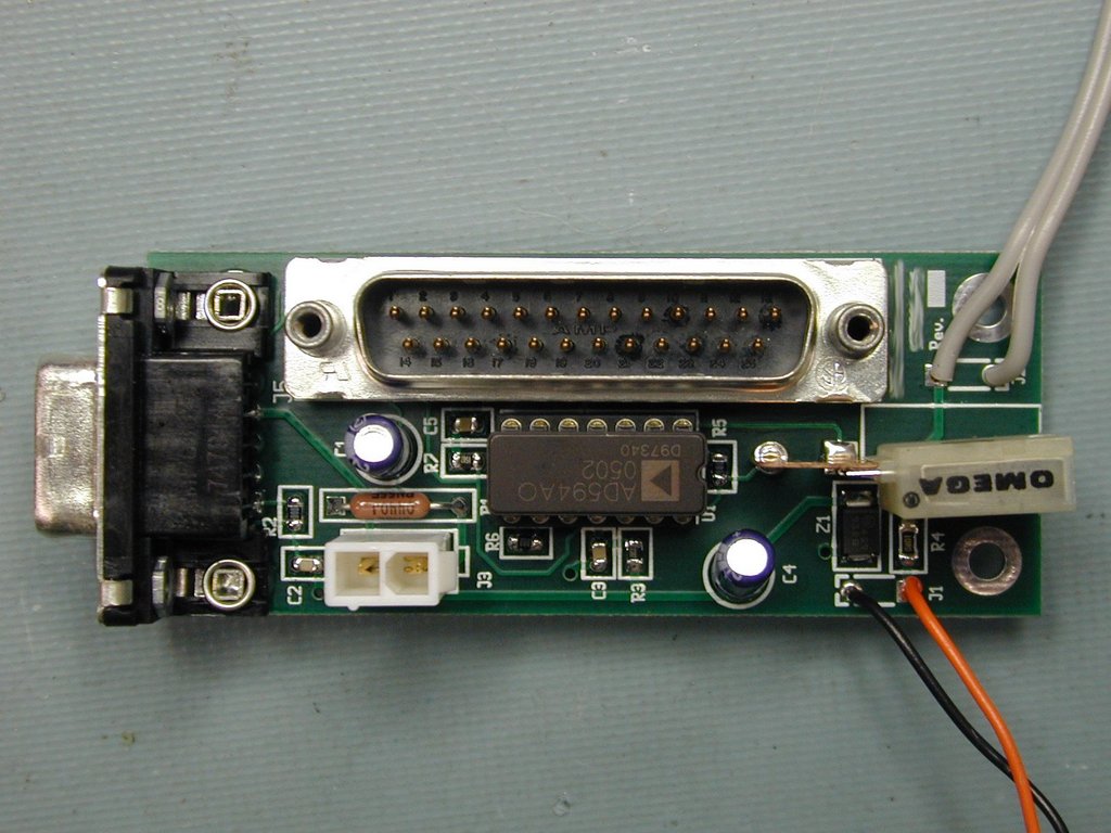
Figure 3. A sensor board created using the gEDA Suite. As is evident, pcb can handle a wide variety of component types.
Resources for this article: /article/8530.
Stuart Brorson has been an avid Linux user since 1994 and became a contributor to the gEDA Project in 2003. By day, Stuart is a professional electrical engineer involved in designing scientific instruments for spectroscopy.