
Porting LinuxBIOS to the AMD SC520: A Follow-up Report
As of July 15, 2005, we have moved the arch repository to Subversion. Arch checkouts will continue to work, but any new changes will be available only in Subversion.
Well, it was too easy. Things were going well with our project to port LinuxBIOS, until we tried to Flash the Flash part. Then we started to hit some problems with the board, the board design and the AMD SC520.
What went wrong? Put simply, when we tried to use the flash_rom program to Flash the part, it failed even to discover the type of part we had on the board. From there, it got worse. We wrote a small program to dump the Flash part, shown here:
#include <errno.h>

#include <fcntl.h>

#include <sys/mman.h>

#include <unistd.h>

#include <stdio.h>

#include <string.h> #

include <stdlib.h>

#include <ctype.h>

main(int argc, char *argv[]) {

int fd_mem;

volatile char *bios;

unsigned long size = 512 * 1024;

int i;

if ((fd_mem = open("/dev/mem", O_SYNC|O_RDWR)) < 0) {

  perror("Can not open /dev/mem");

exit(1);

}

bios = mmap(0, size, PROT_READ, MAP_SHARED, fd_mem,
off_t) (0xffffffff - size + 1));

if (bios == MAP_FAILED) {

perror("Error MMAP /dev/mem");

exit(1);

}

write(1, bios, 512*1024);

}
When we ran this program, we couldn't get sensible results. This program runs and runs well on everything else we own--several thousand K8 nodes, our laptop, 1,500 Xeon nodes--so it is not the program. What's going on?
As mentioned, we found a problem with the design of the MSM586SEG and the other SC520-based boards from Advanced Digital Logic. The problem, put simply, is the full Flash part cannot be accessed from the CPU; only the top 128KB of the part can be accessed. This limitation requires us to modify all of the tools that we support for Flash access, so they are aware that although the nominal size of the Flash is 256 or 512KB, only 128KB of that space is available.
Making that change, however, still did not help. When we dumped the Flash part, we got not garbage but nonsense. We saw strings that read CCCCoooo and so on. This nonsense led us to think that the Flash space was being cached somehow. In addition, we believed the hardware design had a problem such that burst reads from the Flash part--which would happen if the cache were enabled in the range of memory--were returning the same byte four times, not four consecutive bytes.
Then, we hit some other problems. We had two MSM586SEG boards, and the IDE interface on both of them stopped working. It turns out that the MSM586SEG has an FPGA controlling many functions, and we suspect that this FPGA has some teething problems. We decided to try out the older design, the MSM586SEV, which has no FPGA.
The MSM586SEV resolved all our problems save one: we still got nonsense when we tried to read the Flash. It now was time for some deep-diving into the SC520 architecture. We learned that a set of 16 registers, called the PAR registers, need to be managed in order to enable Flashing the part.
What are the PAR registers? They are used to steer memory and I/O access issued by the CPU. Almost all processors today have a special set of registers in the memory and I/O address generation path to modify the manner in which such addresses are handled.
Why is this type of register needed? With multiple busses capable of supporting memory and I/O access, the processor has no idea where to send the access unless it is told. That is the function of the PAR registers. Consider the block diagram of the SC520 shown below.
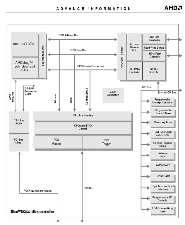
Figure 1. SC520 Block Diagram
A given I/O access can go to the PCI bus or to the GP devices shown at right. A memory access can go to SDRAM, the Flash part or the PCI bus. The PAR registers allow the BIOS to specify, for a given range of I/O or memory, which bus it goes to, whether it is writable or read-only and whether it is cached.
We found that for the BIOS range of memory, 0xe0000-0xfffff, the PAR register was set to SDRAM. This setting is not surprising: for performance, the BIOS typically copies the BIOS image to SDRAM and then makes sure all BIOS code fetches go to the SDRAM holding the BIOS. This operation is commonly called "shadowing the BIOS".
Because Linux doesn't use the BIOS at all, we can ignore this setting. What we do is set the PAR register for the BIOS region, PAR register 15, back to the original BIOS. This is a simple matter of mapping in the registers, and then setting the register. Here is a code fragment to do so:
if ((fd_mem = open("/dev/mem", O_SYNC|O_RDWR)) < 0)

{ perror("Can not open /dev/mem"); exit(1); }

mmcr = mmap(0, 4096, PROT_WRITE|PROT_READ, MAP_SHARED,
fd_mem, (off_t) 0xfffef000);

if (mmcr == MAP_FAILED)

{ perror("Error MMAP /dev/mem"); exit(1); }

p = mmcr + 15; l = *p; printf("l is 0x%lx\n", l);

/* clear cache bits */

l |= (1<<27);

/* enable writeable bit */ l

&= ~(1<<26);

/* set type to flash, not sdram */

l &= ~(7<<29); l |= (4<<29);

/* 64k pages */ l

|= (1<<25);

/* blow away base and size stuff. */

l &= ~(0x1fff | (0x7ff<<14));

printf("l is now 0x%lx\n", l);

l |= (8 << 14) | (0x2000000>>16);

printf("l is now 0x%lx\n", l);

*p = l;
Once we had this done, we still had troubles. The further problem was the design of the PAR registers. They live in memory at 0xfffef000; in other words, they are placed right in the middle of the top 2MB of the 4GB of memory space. This space is, by convention, reserved for BIOS Flash, but the SC520 breaks that convention. So, although we had worked around the board problems, we now were faced with an architectural problem.
A light bulb went off at this point, though, relating to comments we had seen in sample code from AMD. The AMD code always was careful to program the PAR registers to place the Flash part above the top of DRAM, that is, at 32MB or hex 0x2000000. We modified our parbios program slightly, and voilà--all 512KB of Flash now was available, starting at 0x2000000.
Th effects of this change are far-reaching. We had to modify our flash_rom program to enable the Flash on the SC520 and place the Flash at an odd location in memory. Nevertheless, at least we can program it now. This change also affects LinuxBIOS itself. If we want to use all of the Flash part, or simply more then 64KB, we're going to have to make a lot of changes to how LinuxBIOS addresses Flash. We've never seen a machine to date that could not address Flash directly at the top of memory.
The Flash is burned. The serial port works. Let's plug it in.
We also had to modify the SC520 startup code to mimic the setup of the PAR registers. With this set of changes made, we got our first serial output:
LinuxBIOS-1.1.8.0Fallback Tue Jun 14 13:36:22 MDT 2005
starting...

Copying LinuxBIOS to ram.

Jumping to LinuxBIOS
Well, it's a start. For the record, this is version
LinuxBIOS@LinuxBIOS.org--devel/freebios--devel--2.0--patch-45.
What's going on now? What does jumping to LinuxBIOS mean?
What this all means is the ROMCC-based code is working, but the SDRAM is not. Because the SDRAM is not working, the GCC-compiled code doesn't work either. It's time to put in some printing. It's also time to scan carefully the src/cpu/amd/sc520/raminit.c code for errors. As of this version, this code still is pretty ugly, as it came from assembly code. Quick perusal does show a few errors, but prints are the best bet at this point. It is hard to tell what is really going on at times.
Here is the output from this version:
LinuxBIOS-1.1.8.0Fallback Tue Jun 14 16:29:46 MDT 2005
starting...

HI THERE!

sizemem

NOP
And then it resets. For reference, I have committed this version as patch-46. See the raminit code to see where this is blowing up.
At this point, we had to do a bit more digging. We noticed in the AMD assembly code that although a lot of byte registers are used to control various things, some of the assembly seems to use word writes. Even for a byte-wide register that has another register right after it, the code uses word writes.
We moved to word writes and things got much better. Once it is all working, for the sake of cleanliness, we're going to try to turn these back into byte writes. Word writes make no sense, unless there's a hardware problem.
We consistently had resets on a certain code sequence, almost as though we were compiling for the wrong processor. Well, as it happened, we were. Although we had set this line in the Config.lb for the mainboard:
arch i386 end
we had a mistake in one of the extra compilation rules. We were telling ROMCC that the the CPU was a P3:
makerule ./auto.inc depends "$(MAINBOARD)/auto.c
option_table.h ./romcc" action "./romcc -mcpu=p3 -O
-I$(TOP)/src -I. $(CPPFLAGS) $(MAINBOARD)/auto.c -o $@"
end
What's the problem with doing this? In short, when we specify P3 as the CPU for ROMCC, ROMCC generates MMX instructions to use those extra registers. This usage causes trouble, as there are no MMX registers on a 486.
We modified the line as follows:
makerule ./auto.inc depends "$(MAINBOARD)/auto.c
option_table.h ./romcc" action "./romcc -mcpu=i386 -O
-I$(TOP)/src -I. $(CPPFLAGS) $(MAINBOARD)/auto.c -o $@"
end
Things suddenly got much, much better.
But how do we tell? The code that copies the LinuxBIOS RAM part is assembly. It says jumping to LinuxBIOS, but all we see is POST EE. We're going to give you an overview of how you might debug for a new platform. What we're going to do is bypass most of LinuxBIOS that occurs outside of the ROMCC code. Mostly what this code does is uncompress the GCC code and copy it to SDRAM. This code can be hard to follow, however, so we're going to skip it completely.
We're going to make the code that gets copied to RAM be uncompressed rather than compressed, which will take more space. So we need to use as much of the Flash as we can. We're going to need to make Flash map in at 0x2000000. In the auto.c code, we're going to copy that Flash to RAM. Finally, in the code, we're going to insert a few loops like this one:
1: jmp 1b
so that if the machine hangs, we know it got to the infinite loop.
Let's take it one part at a time. In our src/cpu/amd/sc520/raminit.c file, we add the following:
*par++ = 0x8a020200;

/*PAR15: BOOTCS:code:nocache:write:Base 0x2000000, size
    0x80000:*/
You can see that code in there even now. This maps in the FLASH at the 32MB location. Next, we set up LinuxBIOS so that the GCC payload is uncompressed. How do we do this? First, we need to explain memory layout. A number of variables control Flash layout in LinuxBIOS, as shown in Figure 2. Notice that each set of variables can be changed for each payload. In our example, at this point, we are using only one payload, so we show the variables for that case.
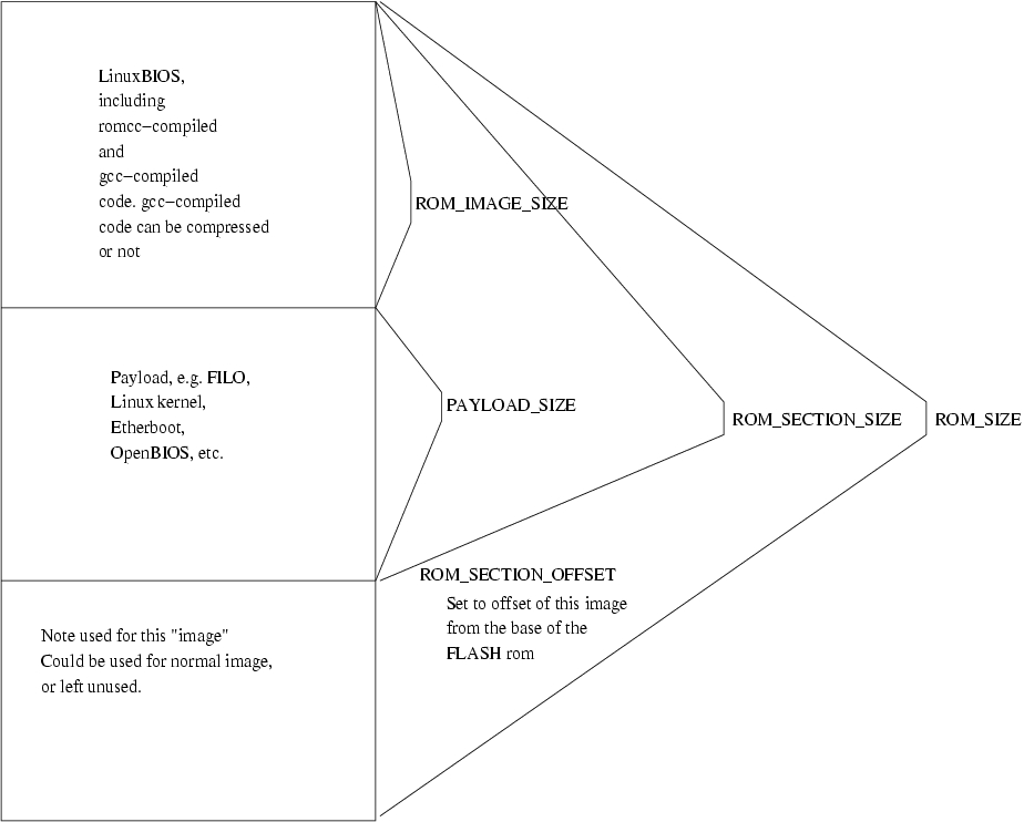
Figure 2. ROM Sizing Controls
In src/mainboard/digitallogic/msm586/Options.lb, we set CONFIG_COMPRESS to zero. We set the ROM_SIZE to 128K, and we set ROM_IMAGE_SIZE large enough to hold the uncompressed payload. If you look at various patch levels of LinuxBIOS in the repository, you can trace our progress in debugging; space does not allow it all here. We've left the appropriate code in auto.c between ifdefs so you can see how it looks. A word of warning: care must be taken with volatile. Romcc is a good compiler. If you're not careful with volatile, it gladly will optimize out copy-assignment loops.
Also, in crt0.s, we did some playing around. Here's a useful assembly sequence for telling you where you are and making sure you get to see it:
_start: movb $0x12, %al ; outb %al, $0x80; jmp _start
We do verify that in the assembly, we're getting to hardware main. So in hardwaremain(), we put in a call to post, followed by a while(1), and we do see the system hang at that point.
The next step is to test a back-to-back post(). In other words, we call post() twice. Why is this important? It verifies that the stack is working too. To this point, all we've done is call functions; we haven't really found out about returns. Calls can work always, but returns rely on a stack that works. If memory is not correctly set up, a return will fail. We have, in the past, had a sequence of function calls that worked fine until the first function exit, at which point the system failed. Memory really can be this tricky. Back-to-back calls to post(), though, verify that we have a working stack.
The key idea here is the careful placement of so-called "halt-and-catch-fire" instructions, with a little bit of output, can allow you to pinpoint how far you are getting in the code.
To make a long story short, we got caught by our own error in the config file. We forgot to tell LinuxBIOS what kind of console we have. This is fixed easily. In src/mainboard/digitallogic/msm586seg/Options.lb, we add:
uses CONFIG_CONSOLE_SERIAL8250

default CONFIG_CONSOLE_SERIAL8250=1
Now, do we have a console? Let's see.
We now get this output:
Copying LinuxBIOS to ram.

Jumping to LinuxBIOS.

LinuxBIOS-1.1.8.0Fallback Wed Jun 22 16:10:58 MDT 2005 booting...

Enumerating buses...

scan_static_bus for Root Device

PCI_DOMAIN: 0000 enabled

scan_static_bus for Root Device done

done

Allocating resources...

Reading resources...

Root Device compute_allocate_io: base: 00000400 size:
00000000 align: 0 gran: 0

Root Device read_resources bus 0 link: 0

PCI_DOMAIN: 0000 missing read_resources

Root Device read_resources bus 0 link: 0 done

Root Device compute_allocate_io: base: 00000400 size:
00000000 align: 0 gran: 0e

Root Device compute_allocate_mem: base: 00000000 size:
00000000 align: 0 gran: 0

Root Device read_resources bus 0 link: 0

PCI_DOMAIN: 0000 missing read_resources

Root Device read_resources bus 0 link: 0 done

Root Device compute_allocate_mem: base: 00000000 size:
00000000 align: 0 gran: e

Done reading resources.

Setting resources...

Root Device compute_allocate_io: base: 00001000 size:
00000000 align: 0 gran: 0

Root Device read_resources bus 0 link: 0

PCI_DOMAIN: 0000 missing read_resources

Root Device read_resources bus 0 link: 0 done

Root Device compute_allocate_io: base: 00001000 size:
00000000 align: 0 gran: 0e

Root Device compute_allocate_mem: base: 100000000 size:
00000000 align: 0 gran:0

Root Device read_resources bus 0 link: 0

PCI_DOMAIN: 0000 missing read_resources

Root Device read_resources bus 0 link: 0 done

Root Device compute_allocate_mem: base: 100000000 size:
00000000 align: 0 gran:e

Root Device assign_resources, bus 0 link: 0

Root Device assign_resources, bus 0 link: 0

Done setting resources.

Done allocating resources.

Enabling resources...

PCI_DOMAIN: 0000 missing enable_resources

done.

Initializing devices...

Root Device init

Devices initialized

Copying IRQ routing tables to 0xf0000...done.

Verifing copy of IRQ routing tables at 0xf0000...done

Checking IRQ routing table consistency...

check_pirq_routing_table() - irq_routing_table located
at: 0x000f0000

done.

Wrote LinuxBIOS table at: 00000500 - 00000af0 checksum 934c

Welcome to elfboot, the open sourced starter.

January 2002, Eric Biederman.

Version 1.3

23:stream_init() - rom_stream: 0xffff0000 - 0xffff7fff

Found ELF candidate at offset 0

header_offset is 0

Try to load at offset 0x0

Could not find a bounce buffer...

Cannot Load ELF Image
Well, that's a start anyway. What's up with the bounce buffer? This is not the real problem. The real problem is LinuxBIOS thinks there is no memory. Remember that in the beginning we set up the CPU with no functions to be called? It turns out we do need to have some functions called, because part of what the functions have to do is indicate how much memory there is. We can look to another Northbridge chip for inspiration. It is pretty close to the SC520 and avoids the complications of the K8 Northbridge, which are very complex. You can see how things now look in the repository, at version 50.
We get a FILO banner and an immediate reset, but at least we get something. Now it's time to turn up the debugging in FILO and see what's wrong.
It turns out that this chip has no hardware timestamp counter (TSC). So when you try to read the TSC, the chip does the right thing; namely, it takes a general protection fault and goes into crash-and-burn mode. FILO never has run before on a chip without a TSC. We had to fix FILO.
We've included a FILO in the Subversion version of the LinuxBIOS tree that can use the SC520 millisecond timer. This timer is a nice free-running timer that provides an accurate timestamp count.
Once we do that, FILO gives us a prompt but says there is no IDE. Another trip back to the MMCR registers shows we need to enable the built-in IDE chip select lines, which are not on by default. Oddly enough, a lot of these embedded chips with built-in controllers tend to come up with those features disabled. Setting a few more MMCR registers by hand does the trick.
As of June 28, we have been booting a Linux kernel. A few more registers needed to be set and then we were good to go.
The kernel comes up and works fine, except not all the interrupts are getting to it. This is a problem in the configuration of the interrupt registers. The interrupt registers are located in the MMCR region of memory, which we previously have had to deal with. Our first idea was to simply dump the registers and restore them, but doing so only made things worse! At that point, not even the clock interrupt worked. Obviously, there is some trickiness to the interrupt register settings that we need to work out.
After a little more looking at the manual, the interrupt issues made more sense. As of July 12, we are booting a kernel to multiuser status, and all interrupts are working.
Well, what's left to do? We're going to add VGA support, so we can have a console. We're going to clean things up in the port, too, now that so much is working. There is not space to track the whole process in this article; we do have a word limit, after all. The board is almost done, and once it basically works, we'll go back and really clean the code up, while leaving in bits that we hope will be useful as debug examples for other ports. We intend to build a lot of computers with these boards; they're pretty nice, albeit a little slow. They're great for building portable development and test clusters, however.
We've also discovered, as we frequently do, that the standard BIOS has misconfigured parts in the chipset. This type of misconfiguration is common with proprietary BIOSes, because nobody can check the correctness of everything they are doing. We're going to need to go back and verify all of our settings now, and make sure that no further mistakes were copied from the proprietary BIOS.
LinuxBIOS is a GPLed system you can use to bring up your boards quickly and reliably. It is in use on over a million systems around the world, in applications as diverse as test instruments and televisions. We use it at LANL (Los Alamos National Laboratory) on almost 5,000 cluster nodes, possibly reaching 7,000 by year's end.
In contrast to proprietary BIOSes, LinuxBIOS lets users tailor the system boot-up sequence to fit their exact needs. The Version 2 system we have shown in these two articles is modular and features an object-oriented structure that, in practice, has let us build compact BIOS images. Images smaller than 32KB are routine, even on complex systems such as 8-way Opterons with 32 PCI busses. LinuxBIOS also is portable and has run on 64-bit Alpha systems as well as PowerPC systems. A port to the PowerPC 970, a 64-bit system, is in progress.
For x86 systems, LinuxBIOS includes a full ANSI C compiler, ROMCC, which uses registers instead of memory.
The SC520 is a great chip marred by almost no mistakes. Probably the single biggest problem is the location of the configuration registers, placed right in the middle of the top 2MB of memory, which always should be reserved for BIOS Flash. That said, the more we worked with this part, the more we appreciate its design.
A lot of our testing of register settings for the SC520 was done in Linux before LinuxBIOS. If you start working on your own port, remember the value of doing this type of register probing under Linux--it's a lot easier. To do I/O operations, use the iopl() system call; for memory operations, use mmap().
Principal work on LinuxBIOS in the coming year will be making it easier for engineers to use it who don't have more than a few days a month to work on it. In other words, we're moving from the dedicated, full-time engineer to the engineer who uses LinuxBIOS as a tool but is not that concerned with the internal workings. The overall goal is to reduce the learning curve for LinuxBIOS. Watch the Web page to see the announcements of these changes as they are made.
Thanks to Gary Karns and Martin Mayer of Advanced Digital Logic for their help in answering questions, expediting board shipments and providing the information we needed to get this all going.
This research was funded in part by the Mathematical Information and Computer Sciences (MICS) Program of the DOE Office of Science and the Los Alamos Computer Science Institute (ASCI Institutes). Los Alamos National Laboratory is operated by the University of California for the National Nuclear Security Administration of the United States Department of Energy under contract W-7405-ENG-36. Los Alamos, NM 87545 LANL LA-UR-05-5272.
Ronald Minnich is the team leader of the Cluster Research Team at Los Alamos National Laboratory. He has worked in cluster computing for longer than he would like to think about.