
An Introduction to IC Design Under Linux
As everyone knows, computers are composed of two main elements, hardware and software. There are many well-known, powerful tools for developing software under Linux. What's not so well-known is that there are also tools available for developing hardware. This article introduces some of the freely-available tools you can use to create integrated circuits (ICs). These tools include: Magic, an IC layout editor; SPICE, an analog circuit simulator and Sigview, a graphical signal viewer. When these programs are used in concert, Linux becomes a platform that can be used to create real-world, working chips.
We'll start by by briefly describing the layout and simulation that are the basis of IC design. Next, we'll cover where and how to get the tools. Then we'll go into more detail about what a chip layout represents. We'll also touch on Magic's technology file, and finish by presenting a complete design example to tie everything together.
In a nutshell, Magic is a graphical tool that a circuit designer uses to specify how an IC should be constructed. This specification is created by drawing rectangles which represent wires and transistors—the building blocks of most ICs. The rectangles are drawn in various colors and fill patterns which represent the layers used to manufacture the chip. (The “layer” concept is explained in more detail below.) The final drawing is usually referred to as the layout of the chip.
Don't be fooled—there's much more to designing an IC than simply making rectangles; otherwise, most any drawing program could do the job. IC design requires further assistance from the software. To that end, Magic is equipped with tools that make IC design easier. For example, it enforces design rules which guarantee that the circuit, as drawn, can be manufactured correctly, and it can extract a list of circuit components and how they're connected (a netlist) from a layout.
These capabilities help provide a basic introduction to Magic and how it's used to do real-world designs. In particular, we'll develop a simple digital circuit—an inverter, which is a ubiquitous building block for complex digital chips.
Magic is used to draw the rectangles in a layout, but how do we know that the circuit corresponding to these rectangles performs as desired? Simulation is a way to verify that the design you've drawn is actually the design you want—it's very much like using a debugger on a piece of software that you're developing. Why bother with simulation? Why not just draw it, build it, and see if it works? Simulation is necessary, because fabricating a chip is costly in a variety of ways. The manufacturing process itself is very expensive, so you want to minimize the number of times you must re-manufacture a defective design. It is also time-consuming, so you want to avoid missing a market window as a result of too many re-manufacturing cycles. Because of these costs, time invested in verifying a design through simulation pays back tremendous dividends.
One tool used to simulate circuit performance is SPICE (Simulation Program with Integrated Circuit Emphasis). Developed at the University of California at Berkeley in the mid-1970's, SPICE and its derivatives, notably PSpice from MicroSim Corporation and HSPICE from Meta-Software, are the most widely-used examples of analog circuit simulators. Using detailed models of the individual circuit components, these programs provide an accurate picture of the device's operation and can analyze many different aspects of a circuit's behavior. Later, we'll look at one aspect that is particularly useful in digital circuit design.
Magic has a WWW page (maintained by Bob Mayo of DEC's Western Research Laboratory) from which you can get source code and browse other relevant information. Point your favorite Web browser to http://www.research.digital.com/wrl/projects/magic/magic.html and follow the “Getting the program and manuals” link. Version 6.5 should be available and out of beta by the time you read this article.
Magic is installed in either the home directory of the user “cad” or the directory pointed to by the environment variable $CAD_HOME. You must either create a “cad” user and make its file space world-readable (assuming you want everyone to be able to run the tools), or designate a directory for the tools and set $CAD_HOME to point to it. We assume you'll choose the second method and refer to the directory specified by $CAD_HOME as the root of the directory tree in which the tools are installed.
After setting $CAD_HOME, untar magic-6.5.tar. Go to the magic-6.5 directory and enter make config. Choose options 1 (X11), 4 (Linux), 5 (Intel based systems, assuming you're on an Intel). Next is a list of optional modules. Leaving them out trades functionality for smaller executable size and compile time. For now, just accept all the optional modules. You can always recompile later if you find you don't use one feature or another. Then, following the instructions on the screen, do a make force to compile everything. After this compile finishes successfully, make install installs everything in the correct location. Don't skip this last step, because Magic depends on having all its support files in the right place.
The latest freely-available version of SPICE is 3f4. Linux-ready sources for SPICE3f4 are available at ftp://ftp.sunsite.edu/pub/Linux/apps/circuits/spice3f4.tar.gz. Compilation and installation instructions are in spice3f4.readme. Note that you must have at least version 1.14.5 of BASH in order to compile. When we compiled ours, we made only one change. We removed the -dWANT_X11 from the conf/linux file, and so did not get the X interface but did get smaller binaries. Since we are using Sigview to look at the the outputs, we don't need this interface anyway. If you don't feel like compiling, an a.out format binary is available at ftp://ftp.eos.ncsu.edu/pub/vlsi/software/Linux/spice3/.
Sigview, developed by Lisa Pickel at MCNC, is an X11-based program for viewing the output of various simulators, including SPICE. By the time this article appears, it should be available at ftp://ftp.sunsite.edu/pub/Linux/apps/circuits/sigview31.tgz. After untarring this file, cd sigview and edit the Makefile. As noted in the instructions at the top, you might need to define SIG_DEV_FILE and SIG_TMP_PATH to point to appropriate places on your system. If they are already set correctly, you can simply use the included (a.out format) executable. If not, a simple make will do the job. You can then place the executable in $CAD_HOME/bin.
Before getting into the details of designing with Magic, it's very helpful to have a basic understanding of the physical structure of an IC and the process by which it's constructed. There are many different types of process technologies—CMOS, GaAs, bipolar and BiCMOS are common ones. Today, CMOS (Complementary Metal Oxide Semiconductor) is the dominant technology for high-density, low-power, low-cost digital circuits; accordingly, we'll focus our examples on designing for CMOS. However, the concepts presented apply equally well to any process.
ICs are constructed by depositing, implanting or growing various materials in patterned layers on a silicon base. Several layers are stacked vertically atop one another; each is separated from the layer immediately above and below by a thin layer of insulating material. It's important to note that a layer can contain many separate objects—for example, it can contain thousands of wires, none of which touch one another.
How do IC manufacturers form the patterns? Typical manufacturing processes are similar to spray-painting, in that they coat the entire IC surface with the material used to make the layer; this obviously precludes the formation of distinct shapes or patterns. If you've ever used a template to spray-paint letters onto a poster or wall, you know that the solution to this problem is to get a piece of shielding, called a mask, cut out the areas you want to paint, and spray through the resulting holes. IC process engineers do the same thing on a vastly smaller scale.
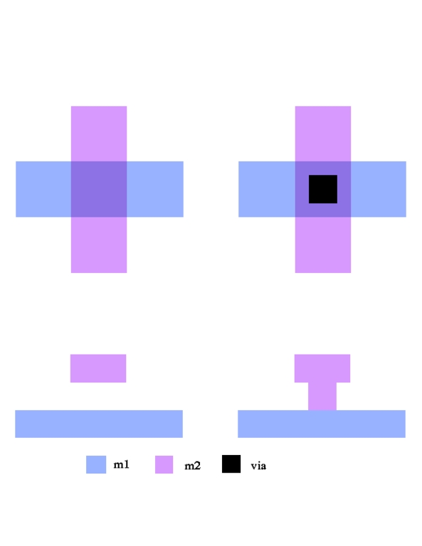
Figure 1. Two Layer Chip Layout
Each step in the fabrication process uses a different mask. Suppose we have a chip with two layers of metal wiring. We'll call the layer closest to the silicon base “m1” and the layer closest to the top “m2”. Because m1 and m2 are different layers, m2 wires can cross over m1 wires without making electrical contact. This is like a high road using an overpass to cross a low road. The left side of Figure 1 illustrates, in both an aerial and cross-sectional view, a vertical m2 wire overlapping a horizontal m1 wire. Note that the two are electrically separate. Suppose now that we want to create a point where a signal can cross from m1 to m2. To build this structure, we need a mask for m1, a mask for m2, and a mask for vias. A via is a hole in the insulating layer, which separates m1 from m2 and allows m2 to flow downward and contact m1, forming an electrical connection. This is shown on the right side of Figure 1; the black square is the via, which connects the two layers. Transistors are more complicated, requiring more masks and different materials.
Magic makes work easier for the designer by hiding much of this underlying physical complexity. Rather than work with mask layers directly, you manipulate abstract layers which implicitly represent one or more masks. For example, to create an m1 to m2 via, rather than draw three shapes on separate mask layers (the m1 layer, the hole layer and the m2 layer), you simply draw one shape on the abstract “via” layer, which has all three mask layers “built-in”. There are also abstract layers having a one-to-one correspondence to mask layers; m1 and m2 are examples. In general, an abstract layer can represent an arbitrary number of mask layers, permitting a great simplification in design.
In order to cram as much as possible onto the IC, modern processes define design rule measurements in microns, mm. A micron is one millionth of a meter. For example, in one particular CMOS process m1 wires must be at least 0.8mm apart from each other and at least 0.6mm wide. Each rule is independent of the others and is specified in fractions of microns.
Magic design rules, on the other hand, are expressed not in microns but in multiples of a unit called lambda, l. Introduced in Carver Mead and Lynn Conway's classic book Introduction to VLSI Systems, lambda is the “quantum” for the rules—all spacings and widths must be multiples of lambda. The previous rules concerning m1 spacing and width would be expressed in terms of lambda as 3<<tt>l and 2[lambda] respectively, where <<tt>l = 0.3<<tt>mm.
Note that using lambda rules is a little costly in terms of area. The spacing rule is now effectively 0.9~<<tt>mm instead of 0.8~<<tt>mm; however, basing rules on lambda allows for scalable designs. The scalable rules allow us to create one design and be confident that it is valid (i.e., it violates no design rules) regardless of the value of lambda. For example, the MOSIS service, which is a low-cost, low-volume IC prototyping service, fabricates chips through several different vendors in various processes. These processes have values of lambda ranging from 0.3<<tt>mm to 1.0<<tt>mm; MOSIS basically has one set of design rules which covers all of these processes. In reality, once lambda starts getting below 0.5~<<tt>mm, even scalable rules change somewhat, but this is a detail. These rules are referred to as the SCMOS (Scalable CMOS) rules, and we use them in our design example.
As mentioned earlier, there are several different IC process technologies. Magic is technology-independent and can be used with all. The information that Magic needs about the target process resides in an external file called the technology file (tech file), which Magic reads when the program starts. By default Magic looks in $CAD_HOME/lib/magic/sys for the file scmos.tech27. Both the location and name of the tech file can be specified on the command line with the -T switch, although the name of the tech file must end with a “.tech27” extension. For example, to use the scmos-sub.tech27 tech file, you type magic -T scmos-sub.
Included with the Magic distribution in the scmos directory are multiple tech files for various processes offered by MOSIS. As mentioned above, when lambda gets very small, the design rules begin to change. MOSIS provides different tech files to account for this.
Items defined in the tech file include:
layer definitions (e.g., names, colors) and how layers interact with one another
design rules
device (transistor) geometry and parasitics
instructions on how to convert Magic's abstract layers to mask layers and vice versa
Knowing the tech file internals isn't necessary to use Magic; in fact, unless you're writing a tech file for a new process or modifying one for an existing process, you can think of the tech file as a “black box”. If you're interested, you can find a complete discussion of the tech file format in Magic Maintainer's Manual #2: The Technology File, located in the doc subdirectory of the Magic source tree.
We now pull it all together with a real-world design example—an inverter. An inverter simply flips a bit; it turns a 1 into a 0 and a 0 into a 1. This may sound trivial, but it's an essential building block for more complex digital circuits.
First, we'll walk through the layout and design rule check (DRC) of the inverter, explaining things as we go. Then we'll extract the netlist and simulate the chip using SPICE. After we're convinced the chip works properly, we'll construct the CIF file to send to the foundry to have the chip fabricated.
Although this example is very rudimentary, you can find much more complete documentation in the Magic Tutorial series, located in the doc subdirectory of the Magic source distribution. These excellent tutorials cover both the basics and more advanced usage (such as hierarchical design, multiple windows and interactive routing) that isn't covered here.
First, invoke Magic from your shell prompt. Let's call our example file “inverter”. We'll use the default tech file, so we don't need to specify one with the -T switch.
magic inverter
A new layout window appears in which you design your chip; error messages and feedback appear in the window in which you started Magic (the command window). Magic handles window focus a little differently than you might expect—even though the input focus remains on the layout window, anything you type appears in the command window. Many commands work regardless of which window has the focus. When everything is ready, Magic displays a prompt in the command window.
The first thing to do is “paint” the two metal wires that supply current to the inverter—these wires are called the power rails. To create the first rail, make sure the focus is in the layout window, and type the following commands (the colon in the first column is required):
:grid
:box 0 0 4 5
:paint m1
The first command simply turns on the reference grid, although we're zoomed too far out to see it right now. The second command changes the shape of the box so that the lower-left corner is at (0,0) and the upper-right corner is at (4,5). The third command fills the box with blue paint that represents the first layer of metal. The box is the center of attention; most operations, such as painting and erasing, affect only the area within the box.
Now zoom in to get a clearer picture:
:box 0 0 12 32
Instead of typing a long command, we use a macro. Simply press the z without the colon, and the layout window zooms to the box. Note that after zooming the reference grid appears; each hash mark represents one lambda. Shortcuts like this are very handy, so let's explore them some more.
A macro is a single keystroke not preceded by a colon. It can represent any arbitrary sequence of typed commands; for example, the z above represents the :findbox zoom command. System-wide macros are read at start-up from the file $CAD_HOME/lib/magic/sys/.magic. You can define you own macros in a .magic file in your home directories. And you can define macros at any time by entering:
:macro <key> <action to perform>
The mouse provides a quick way to both move and resize the box as well as paint. Move the cursor around the layout window and click the left mouse button as you do. This action moves the box so that its lower-left corner (the anchor point) is placed at the spot where you clicked. Now move the cursor around while clicking the right mouse button. The corner opposite the anchor point is placed where you let the button up. Notice this might result in the anchor point moving, since it's always the lower-left corner of the box.
To see how the mouse makes painting easier, first enter:
:box 0 27 4 32
to move the box where we want the second rail. Normally, you'd use the mouse to move and resize instead of typing a box command, but we want to make sure we all have the box in the exact same location. Now instead of typing :paint m1, move the cursor over the existing m1 rectangle and click the middle mouse button (for those of you using a 2-button mouse, click both buttons simultaneously). The box is now filled with metal 1. Clicking the middle button fills the box with whatever paint layers are underneath the cursor when you click. This leads to a simple way to erase any paint in the box—place the cursor over empty background and click the middle button, which paints “nothing” into the box.
Like any good editor, Magic has an undo facility for those times when you make a mistake or just want to try something out without having to commit. The u macro undoes the last action while the U macro implements the redo command. It's not unlimited; expect only the last 10 actions or so to be undoable. However, it's more than enough to let you erase a few rectangles and get them back.
A CMOS inverter has two Field-Effect Transistors, one p-type (PFET) and one n-type (NFET). Transistors are constructed by drawing polysilicon (or poly, for short) over diffusion. There are two types of diffusion, p and n. A PFET is poly over p-diffusion; an NFET is poly over n-diffusion.
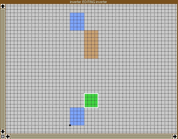
Now let's start drawing the transistors. Position the box at ll (lower left) = (4,19), ur (upper right) = (8,27) and type:
:pai pdiff
Magic understands abbreviations for commands, such as pai for paint. The layer pdiff is p-type diffusion; each layer can have multiple names defined in the tech file. In SCMOS, p-diffusion can be called pdiffusion, pdiff or brown.
Now it's time for the n-diffusion. Place the box at ll=(4,5) and ur=(8,9) and type:
:pai ndiff
At this point your layout should look like the one in Figure 2. If not, you've gone astray; use the undo command and try again.
Figure 2. Layout Showing Diffusions Only
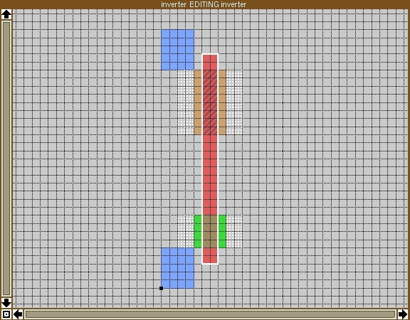
The transistors need poly running over the diffusion. In an inverter, the two polys for the transistors are connected together. This is the inverter's input—the signal driving the inverter is connected to the poly. It's simplest, then, to draw a single piece of poly which crosses both diffusions. Place the box at ll=(5,3) and ur=(7,29) and type:
:pai poly
Your layout should then look like Figure 3.
Figure 3. Layout Showing Polysilicon Crossing Diffusions to Define Transistors
There are a couple of important points to notice. First, the area where the poly crosses the diffusion has a diagonally-striped pattern different from both poly and diffusion. This area represents the actual transistor, since FETs are constructed wherever poly passes over diffusion. To see this, place the cursor over the top transistor, and select it by pressing the s key. Now enter :what, which displays the names of the selected paint. Here, the selected area is “ptransistor”; Magic actually changes the paint from pdiffusion to ptransistor when poly crosses over it. The same concept applies when poly crosses over n-diffusion to form an “ntransistor”.
The other, very important thing to notice in Figure 3 is that white dots suddenly appear. If you work with Magic, get used to these dots—they indicate design rule violations, which Magic always checks for whenever something changes. To see which rule has been violated, place the box over the error dots, and use the y macro, which represents the :drc why command. Magic prints the reason for the error in the command window:
Diffusion must overhang transistor by at least 3 (MOSIS rule #3.4)
Since the overhang is only 1, we get design rule violations. Notice the dots occur only in the area that causes the error.
Now that we know what the problems are, let's fix them. Move the box to ll=(2,19) and ur=(10,27) to contain the upper error dots and type :pai pdiff. The error disappears. Now color the area in ndiffusion to eliminate the remaining errors. The layout now contains two “DRC-clean” transistors—no error dots are now displayed.
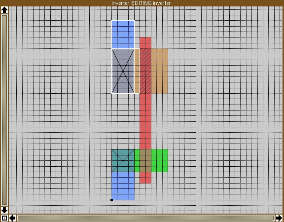
To see which components are connected to a particular rectangle, place the cursor over it and press the s key twice quickly. The first key press selects the rectangle; the second selects everything that's electrically connected to it. Try this on either metal rail, and notice that they are both electrically isolated from everything else. The top rail must connect to the diffusion on one side of the PFET and the bottom rail to the diffusion on one side of the NFET; otherwise, no current can flow. Thus, we need what's called a diffusion-to-m1 contact, abbreviated pdc or ndc depending on whether we're talking about p or n diffusion respectively.
Place the box at ll=(0,5), ur=(4,9) and type :pai ndc. Now make a pdc at ll=(0,19) and ur=(4,27). Checking connectivity shows that the rails are connected to both the adjacent contacts and the diffusion right up to, but not including, the transistor. At this point, check your layout against Figure 4.
Figure 4. Layout with Electrical Connections Added
Now for the output. In a CMOS inverter, the output is made by connecting together the sides of the transistors that are not connected to a rail. Place the box at ll=(8,5) and ur=(12,9) and paint an ndc (try doing this using the middle mouse button). Then put the box at ll=(8,19) and ur=(12,27) and paint a pdc. To connect these two contacts together, we need m1 between them: put the box at ll=(8,9) and ur=(12,19) and paint m1. Check the connectivity of the output to verify that the two contacts are tied together.
Congratulations. You've just drawn the layout for a fully-functional CMOS logic gate—however, we're not quite finished.
Labeling assigns a name to a specified rectangle in the layout and thereby to every rectangle electrically connected to it. Labeling serves two purposes. First, it's like commenting code in that it lets you know what signals are where. Second, it makes simulation much easier when you pick sensible names rather than generate them automatically; for automatically, “input” is much easier to remember than “a_43_n15#”.
Let's label the rails first. Select the upper rail by moving the cursor over it and pressing the s key. Then type:
:label Vdd
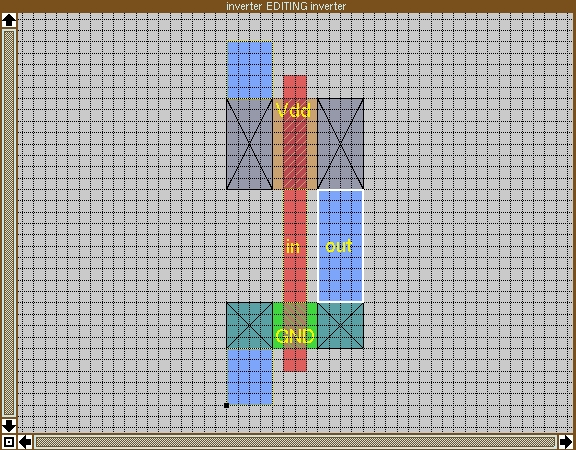
“Vdd” should appear next to the rail. Select the other rail and type :lab Gnd. Notice the labels are placed somewhat randomly. Now select the poly between the two transistors and type :lab in center. This places the label in the middle of the selected rectangle. Finally, select the output m1 and type :lab out center. The now-finished layout should look like Figure 5.
Figure 5. Completed Layout with Labels
To save your layout, type :save. If you want to save it under another name, simply type the name too; e.g., :save newcellname. Magic automatically appends a .mag extension.
The next step is to simulate the layout to verify that it works correctly. Magic's .mag files are stored simply as a collection of various types of rectangles, but simulators require a netlist of circuit components, such as transistors and capacitors. Recall that a netlist is a list of circuit components and how they're connected.
You use Magic itself to extract a netlist from a layout. Magic's extractor recognizes various combinations of rectangles as defined in the tech file and converts them into the appropriate circuit elements. It also extracts connectivity between shapes, thus making a complete netlist.
You must choose an “extraction style”, which tells Magic how to interpret the shapes in the layout. To see the available styles, type :extract style. For our purposes, the important part of the style name is the number, which refers to the minimum transistor length. For example, in the lambda=1.0(scna20_orb) style we'll use, this length is 2.0mm. This should be the current style; if it's not, enter:
:extract style lambda=1.0(scna20_orb)
To complete the extraction, simply type :extract. Magic makes an inverter.ext file. This file is an intermediate description of the circuit containing all the information necessary to build a netlist for various simulators. We're now ready to begin simulation, so quit magic by entering :quit.
Before beginning a simulation, first create a SPICE file and add transistor models and SPICE commands to it. Next, simulate the inverter to verify that it was laid out correctly.
First, translate the inverter.ext file into something that SPICE can understand. The ext2spice program by Stefanos Sidiropolous that comes with the Magic distribution performs this translation. Simply enter:
ext2spice -f spice3 inverter.ext
We specify “spice3” format output, because earlier SPICE versions can't handle text strings for labels.
We now have a file that SPICE can understand, but it's incomplete in an important way. For SPICE to simulate a device correctly, it needs a model, a mathematical description of the device's behavior. In particular, we now need models for the two transistors (n-type and p-type) that we've used in our design.
SPICE has a variety of built-in transistor models specified in terms of sets of parameters. These parameters vary according to the fabrication process used, so it's up to the user to specify the correct parameters for the process being used. Fortunately, you don't have to figure these out yourselves—you can get them from MOSIS at ftp://ftp.mosis.edu/pub/mosis/vendors/orbit-scna20. This FTP site contains a whole slew of data from past runs; we chose a typical one from the “Level 2 Parameters” section. One minor detail—note that you need to change the “CMOSN” and “CMOSP” to match ext2spice's output, “NFET” and “PFET”.
After pasting in the transistor models, the inverter.spice file should look like Listing 1.
We've drawn the inverter and extracted a netlist. Now we need to simulate the chip to make sure it'll perform as expected when the chip is fabricated. A simulator such as SPICE can do many different types of circuit analysis. We will demonstrate two that are very useful for the digital circuit designer.
It might seem curious to use an analog circuit simulator for a digital circuit. We think of digital circuits as being in one of two states, 0 or 1, while analog circuits can take any of a continuous range of values. What's important to realize is that a digital circuit is actually a special kind of analog circuit. At the circuit level, a signal is either a voltage or current, and these are really analog quantities. The conventional 0 and 1 representations of a bit are simply abstractions of two particular voltage values; the actual values depend on the process in which the chip is fabricated. With CMOS in particular, you can generally ignore the currents and deal only with the voltages, due to the FET's mode of operation. For example, in the particular process for which we extracted our inverter, a 1 corresponds to 5 Volts (5V). In other processes, it might correspond to 3.3V or 2.5V. Happily enough, a 0 generally means 0V. As we all know, digital circuits don't switch instantaneously between their two values. It takes time to change voltages, and this delay is one of the things that makes your CPU run at 100MHz instead of 133MHz.
The upshot is that SPICE simulates analog behavior, but as digital circuit designers, we will interpret the circuit's output as digital bits rather than the analog voltages they actually are.
Simulators specialized for digital circuits do not provide the level of detail, that is, accuracy, that SPICE does, but they are orders of magnitude faster. IRSIM, which is available through the Magic WWW home page (see Resources at the end of the article) is an example of such a simulator.
Suppose we apply the test vector 101 to the inverter over a period of 75 nanoseconds (1 ns = 10-9 seconds). How will the output change over this time interval? To answer this question, SPICE can do a transient analysis. In a transient analysis, you define the input signal(s) and tell SPICE to simulate the circuit for a certain amount of time from the circuit's point-of-view, not real time. A transient analysis provides timing information, for example, how long the output takes to switch from 1 to 0. This analysis is also useful for verifying the circuit's functionality; you simply apply the test vector and check the output for correctness.
Let's apply the vector 101 to our inverter. Add the following lines to the end of the inverter.spice file:
Vpwr Vdd Gnd 5
Vgnd Gnd 0 0
Vinput in Gnd 0 PULSE( 0V 5V 0ns 2.5ns 2.5ns 25ns 50ns )
 .TRAN 0.1ns 75ns
 .end
Let's go over this specification line-by-line. Line 1 defines a 5V voltage source between Vdd and Gnd; this is the power supply. Line 2 is necessary because of a SPICE artifact of always referring to ground as 0. We simply tie Gnd and 0 together (electrically speaking) by using a 0V voltage source, i.e., a short-circuit. Line 3 defines a voltage source between “in” and ground; this is the inverter's input. Looking at the parameters in parentheses, we have a voltage source whose initial voltage is 0V and “pulsed” voltage is 5V, and it starts after a 0ns delay. It has a rise time (i.e., the time required to switch from 0 to 1) of 2.5ns, and a fall time (i.e., the time required to switch from 1 to 0) also of 2.5ns. The width of each pulse is 25ns, and it repeats after 50ns have elapsed. Line 4 means that we want to do a transient analysis with a resolution of 0.1ns that lasts for 75ns. Line 5 ends the circuit file. Save the file, then run the simulation by typing:
spice3 -r inverter.out < inverter.spiceNow, let's view the results by typing:
sigview inverter.outWe're interested only in the top two signals, “out” and “in”, as shown in Figure 6.
Figure 6. SPICE Inverter Output
From the digital point-of-view we see that the inverter correctly produces a 010 pattern; from the analog point-of-view we see that the output's rise time is about 0.91ns and its fall time is about 0.89ns.
At this point, the layout is completed and verified, and it's time to send it off to the foundry to be manufactured. Since Magic files don't contain any information about physical dimensions (remember, all measurements are in terms of lambda), we need to create a file that gives the layout's shapes definite sizes in terms of microns. Also, since this file is used by the foundry to pattern the masks used to make the chip, it specifies shapes in terms of mask layers instead of Magic's abstract layers. Magic understands two file formats for describing physical geometries, CIF (Caltech Intermediate Format) and Calma GDS-II; MOSIS accepts both. We arbitrarily chose CIF for our example.
Just as there are several extraction styles, there are several CIF styles. The first thing we need to do is specify the correct one. Launch Magic again with the inverter file (type magic inverter at the shell prompt), and then type :cif ostyle to see a list of available CIF output styles. The current style should be lambda=1.0(nwell); if it's not, make it so by typing :cif ostyle lambda=1.0(nwell).
Creating the CIF file is simple; type :cif write inverter. This creates the file inverter.cif, which we'd send to MOSIS. This process is referred to as “tapeout”, a term coined before the advent of FTP when IC designs were stored on magnetic tape. If this were a real design, you would now take to your bed to make up for the fact that you hadn't slept in the last three weeks.
We've introduced three powerful tools for IC design under Linux:
Magic, for creating layouts
SPICE, for simulating circuits extracted from the layouts
Sigview, for viewing the results of SPICE simulations.
With these tools, a designer can create working, commercial-quality chips without spending lots of money on a workstation and CAD software.
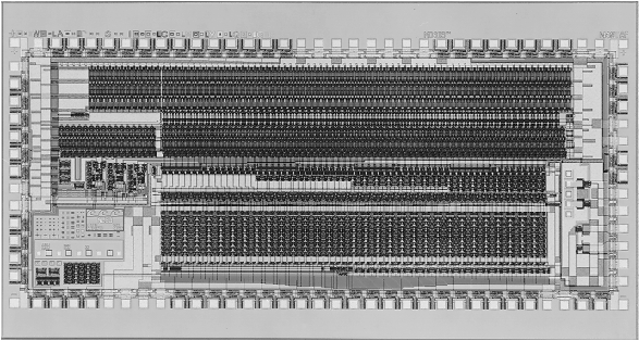
The design example we used to demonstrate these tools was small but not useless. In fact, Figure 7 shows a 32,701-transistor IC measuring 2.71mm by 6.15mm, designed with Magic, that uses building blocks very much like the inverter we just made. (This may sound like a lot of transistors, until you consider that current commercial microprocessors are rapidly approaching 10 million transistors on a chip smaller than 2cm by 2cm.)
Thanks for making it this far. Obviously, there's a lot we've left out about the complexities of hardware design. However, we have demonstrated that Linux can be used for developing hardware as well as software. Perhaps the “SuperGizmo 6000” will be designed on the Linux boxes of the future.
We've barely scratched the surface of IC design. If you're interested in exploring this area further, you'll want to consult some references. We have used and can recommend the books listed in the Resources box.


